Certified by


Capabilities
01
04
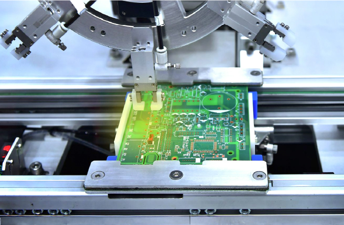
Precision HDI PCB Manufacturing for Medical Devices
Et est admodum mirum videre plebem innumeram mentibus ardore quodam infuso cum dimicationum curulium eventu pendentem. haec similiaque memorabile nihil vel serium agi Romae permittunt. ergo redeundum ad textum.